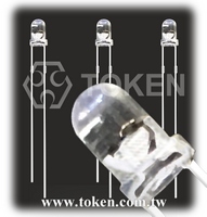
Ambient Light Sensing Phototransistors IR (PT-A2-AC-850)
Ambient Light Sensing Phototransistors IR (PT-A2-AC-850)
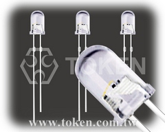
With RoHs compliant, Token phototransistors are available in a wide range of packages.
A phototransistor is known as a device in which turns light source energy into electric energy. Phototransistors are very close to photoresistors but produce both current and voltage, while photoresistors simply produce current. The reason is a phototransistor includes a bipolar semiconductor and targets the energy this can be transmitted via it.
Phototransistors are light-sensitive transistors. A common type of phototransistor resembles a bipolar transistor with its base lead removed and replaced with a light-sensitive area. This is why a phototransistor has only 2 terminals instead of the usual 3. However, when the light-sensitive region is exposed to light, a small base current is generated that controls a much larger collector-to-emitter current.
Token PT-A2-AC-850 family with environmentally friendly photosensitive sensors, control sensitivity under low illumination, stable current signal output under strong light source. Multiple light at the same time can be used to ensure consistent photosensitive effect, not false trigger. Meet the latest environmental requirements of toys. Applicable to all kinds of light control lighting products (such as night lights, lawn lamps, solar lights, etc.), automatically adjust the background light (such as LCD, mobile phones, cameras, computer cameras, security monitoring machines, etc.).
The PT-A2-AC-850 ambient light sensor, commonly used in infrared reception, Ultra-thin multi-point infrared touch screen, and all kinds of high-light or visible light interference strong products, such as various types of infrared light control, infrared on the radio, infrared reflection and other electronic products.
For the convenience of installation in all kinds of products in any position, different sizes are available upon request. So that product consistency is better, more market competitiveness. It is also achievable to provide the bright current / dark current (bright resistance / dark resistance) for the most suitable product.
Download complete specification Ambient Light Sensing Phototransistors IR (PT-A2-AC-850) PDF.
- Good batch consistency, small static current.
- Fast response speed, stable performance, beautiful appearance.
- The effective control distance is greater than 1.5 meters.
- Low current loss in the static.
- Replace the traditional CDS photoresistor.
- Cadmium and lead free with RoHS compliant.
- Applicable to control all kinds of light control toys and Infrared testing equipment.
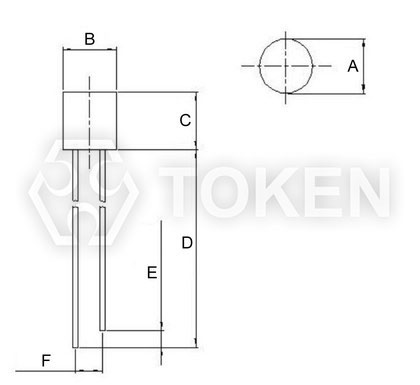
Dimensions & Configurations (Unit: mm) (PT-A2-AC-3-BE-850) & (PT-A2-AC-5-BE-850) Bullet Edge
|
||||||||||
| Part NO. | A (mm) | B (mm) | C (mm) | D (mm) | E (mm) | F (mm) | G (mm) | H (mm) | I (mm) | |
| PT-A2-AC-3-BE-850 | 3.85 ± 0.20 | 3.00 ± 0.20 | 1.50 Max. | 1.50 ± 0.5 | 2.54 ± 0.20 | 5.30 ± 0.20 | 1.00 ± 0.20 | 25.4 Min. | 0.50 ± 0.20 | |
| PT-A2-AC-5-BE-850 | 5.80 ± 0.20 | 5.00 ± 0.20 | 1.50 Max. | 1.50 ± 0.5 | 2.54 ± 0.20 | 8.70 ± 0.20 | 1.00 ± 0.20 | 25.4 Min. | 0.50 ± 0.20 | |
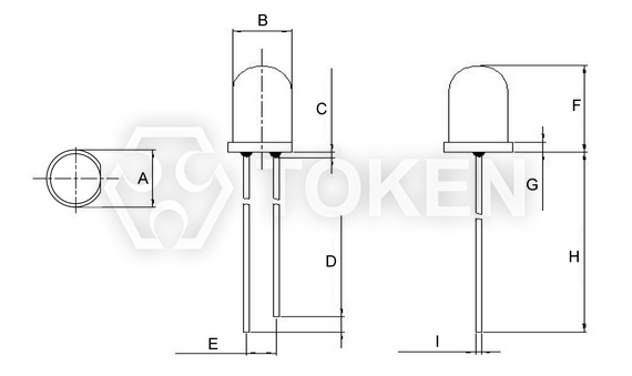
- The epoxy resin highest: 1.5mm max.
- Product images, plastic color of apperence, and all other information is for reference only, goods in-kind prevail.
- Short Lead—Collector Long Lead—Emitter.
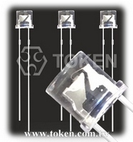
Dimensions & Configurations (Unit: mm) (PT-A2-AC-5-PE-850) Plate Edge
|
||||||||||
| Part NO. | A (mm) | B (mm) | C (mm) | D (mm) | E (mm) | F (mm) | G (mm) | H (mm) | I (mm) | |
| PT-A2-AC-5-PE-850 | 5.80 ± 0.20 | 5.00 ± 0.20 | 1.50 Max. | 1.50 ± 0.5 | 2.54 ± 0.20 | 5.30 ± 0.20 | 1.00 ± 0.20 | 25.4 Min. | 0.50 ± 0.20 | |

- The epoxy resin highest: 1.5mm max.
- Product images, plastic color of apperence, and all other information is for reference only, goods in-kind prevail.
- Short Lead—Collector Long Lead—Emitter.
Dimensions & Configurations (Unit: mm) (PT-A2-AC-5-PN-850) Plate None
|
|||||||||||
| Part NO. | A (mm) | B (mm) | C (mm) | D (mm) | E (mm) | F (mm) | |||||
| PT-A2-AC-5-PN-850 | 5.00 ± 0.20 | 5.00 ± 0.20 | 5.30 ± 0.20 | 25.4 Min. | 1.50 ± 0.50 | 2.54 ± 0.20 | |||||
- The epoxy resin highest: 1.5mm max.
- Product images, plastic color of apperence, and all other information is for reference only, goods in-kind prevail.
- Short Lead—Collector Long Lead—Emitter.
Electro-Optical Characteristics (Ta=25°C) (PT-A2-AC-3-BE-850) Bullet Edge
| Parameter | Symbol | Condition | Min. | Typ. | Max. | Unit |
| Peak Wavelength | λp | \ | - | 850 | - | nm |
| Spectral Response Bandwidth | λ | \ | 400 | - | 1100 | nm |
| Collector-Emitter Breakdown Voltage | Bvceo | Ice=100µA Ee=0mW/cm2 |
30 | - | - | V |
| Emitter-Base Breakdown Voltage | Bveco | Ice=100µA Ee=0mW/cm2 |
6 | - | - | V |
| Collector-Emitter Saturation Voltage | Vce (sat) |
Ice=2mA Ee=1mW/cm2 |
- | - | 0.4 | V |
| Photo Current | IL(1) | Vcc=5V Ev=10Lux |
15 | 30 | 45 | μA |
| IL(2) | Vcc=5V Ev=30Lux |
45 | 90 | 145 | μA | |
| IL(3) | Vcc=5V Ev=100Lux |
150 | 300 | 450 | μA | |
| Collector Dark Current | Iceo | Vce=5V Ev=0Lux |
- | - | 0.1 | μA |
| Rise Time | tr | Vcc=5V Ice=1mA RL=1000Ω |
15 | μs | ||
| Fall Time | tf | 15 | ||||
Electro-Optical Characteristics (Ta=25°C) (PT-A2-AC-5-BE-850) Bullet Edge
| Parameter | Symbol | Condition | Min. | Typ. | Max. | Unit |
| Peak Wavelength | λp | \ | - | 850 | - | nm |
| Spectral Response Bandwidth | λ | \ | 400 | - | 1100 | nm |
| Collector-Emitter Breakdown Voltage | Bvceo | Ice=100µA Ee=0mW/cm2 |
30 | - | - | V |
| Emitter-Base Breakdown Voltage | Bveco | Ice=100µA Ee=0mW/cm2 |
6 | - | - | V |
| Collector-Emitter Saturation Voltage | Vce (sat) |
Ice=2mA Ee=1mW/cm2 |
- | - | 0.4 | V |
| Photo Current | IL(1) | Vcc=5V Ev=10Lux |
30 | 50 | 90 | μA |
| IL(2) | Vcc=5V Ev=30Lux |
90 | 150 | 270 | μA | |
| IL(3) | Vcc=5V Ev=100Lux |
300 | 500 | 900 | μA | |
| Collector Dark Current | Iceo | Vce=5V Ev=0Lux |
- | - | 0.1 | μA |
| Rise Time | tr | Vcc=5V Ice=1mA RL=1000Ω |
15 | μs | ||
| Fall Time | tf | 15 | ||||
Electro-Optical Characteristics (Ta=25°C) (PT-A2-AC-5-PE-850) Plate Edge
| Parameter | Symbol | Condition | Min. | Typ. | Max. | Unit |
| Peak Wavelength | λp | \ | - | 850 | - | nm |
| Spectral Response Bandwidth | λ | \ | 400 | - | 1100 | nm |
| Collector-Emitter Breakdown Voltage | Bvceo | Ice=100µA Ee=0mW/cm2 |
30 | - | - | V |
| Emitter-Base Breakdown Voltage | Bveco | Ice=100µA Ee=0mW/cm2 |
6 | - | - | V |
| Collector-Emitter Saturation Voltage | Vce (sat) |
Ice=2mA Ee=1mW/cm2 |
- | - | 0.4 | V |
| Photo Current | IL(1) | Vcc=5V Ev=10Lux |
1.5 | 3 | 4.5 | μA |
| IL(2) | Vcc=5V Ev=30Lux |
4.5 | 9 | 13.5 | μA | |
| IL(3) | Vcc=5V Ev=100Lux |
15 | 30 | 45 | μA | |
| Collector Dark Current | Iceo | Vce=5V Ev=0Lux |
- | - | 0.1 | μA |
| Rise Time | tr | Vcc=5V Ice=1mA RL=1000Ω |
15 | μs | ||
| Fall Time | tf | 15 | ||||
Electro-Optical Characteristics (Ta=25°C) (PT-A4-AC-5-PN-850) Plate None
| Parameter | Symbol | Condition | Min. | Typ. | Max. | Unit |
| Peak Wavelength | λp | \ | - | 850 | - | nm |
| Spectral Response Bandwidth | λ | \ | 400 | - | 1100 | nm |
| Collector-Emitter Breakdown Voltage | Bvceo | Ice=100µA Ee=0mW/cm2 |
30 | - | - | V |
| Emitter-Base Breakdown Voltage | Bveco | Ice=100µA Ee=0mW/cm2 |
6 | - | - | V |
| Collector-Emitter Saturation Voltage | Vce (sat) |
Ice=2mA Ee=1mW/cm2 |
- | - | 0.4 | V |
| Photo Current | IL(1) | Vcc=5V Ev=10Lux |
1.5 | 3 | 4.5 | μA |
| IL(2) | Vcc=5V Ev=30Lux |
4.5 | 9 | 13.5 | μA | |
| IL(3) | Vcc=5V Ev=100Lux |
15 | 30 | 45 | μA | |
| Collector Dark Current | Iceo | Vce=5V Ev=0Lux |
- | - | 0.1 | μA |
| Rise Time | tr | Vcc=5V Ice=1mA RL=1000Ω |
15 | μs | ||
| Fall Time | tf | 15 | ||||
Absolute maximum ratings (Ta=25°C) (PT-A2-AC)
| Parameter | Symbol | Value | Unit |
| Collector-Emitter Voltage | VCEO | 30 | V |
| Emitter-Collector-Voltage | VECO | 6 | V |
| Power Dissipation | PC | 70 | mW |
| Operating Temperature Range | Topr | -25 ~ +85 | °C |
| Storage Temperature | Tstg | -40 ~ +100 | °C |
Relative Spectral Sensitivity vs. Wavelength (PT-A2-AC-3-BE-850)
|

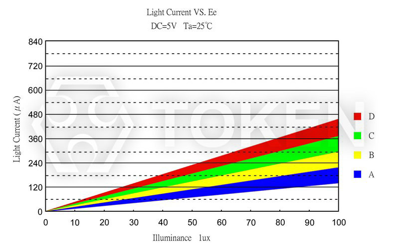
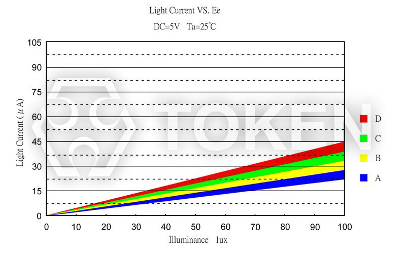
Photo Current vs. Illuminance (PT-A2-AC-3-BE-850)
|
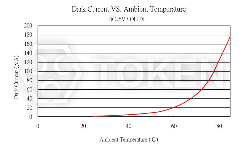
Dark Current vs. Ambient Temperature (PT-A2-AC-3-BE-850)
|

Relative Spectral Sensitivity vs. Wavelength (PT-A2-AC-5-BE-850)
|

Photo Current vs. Illuminance (PT-A2-AC-5-BE-850)
|
Dark Current vs. Ambient Temperature (PT-A2-AC-5-BE-850)
|
Relative Spectral Sensitivity vs. Wavelength (PT-A2-AC-5-PE-850)
|
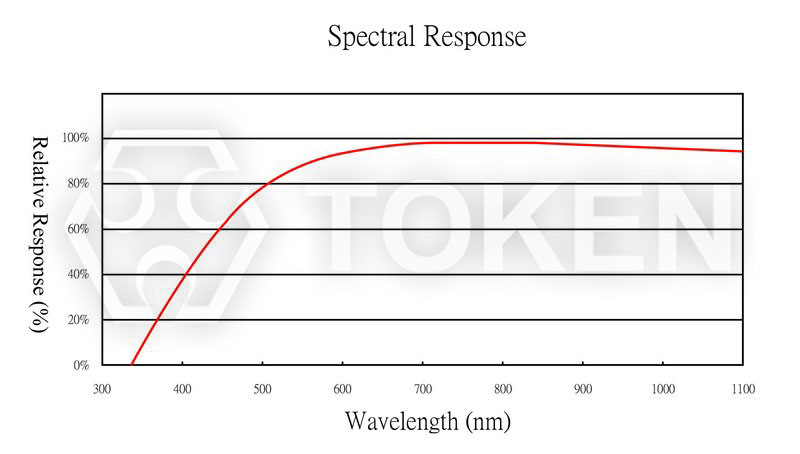
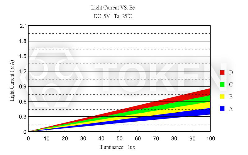
Photo Current vs. Illuminance (PT-A2-AC-5-PE-850)
|

Dark Current vs. Ambient Temperature (PT-A2-AC-5-PE-850)
|

Relative Spectral Sensitivity vs. Wavelength (PT-A2-AC-5-PN-850)
|
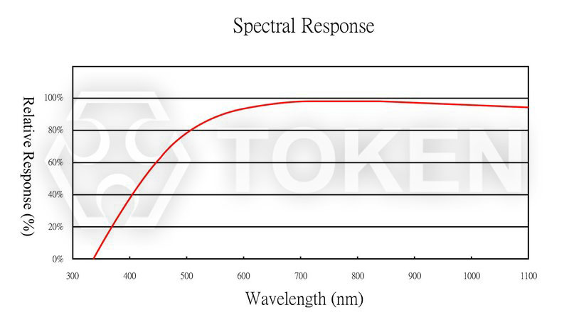
Photo Current vs. Illuminance (PT-A2-AC-5-PN-850)
|
Dark Current vs. Ambient Temperature (PT-A2-AC-5-PN-850)
|

Bullet Edge Phototransistor (PT-BE) Precaution Usage
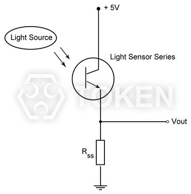
Photo Current Measurement Method (PT-BE)
Lead-forming and cuttings:
- Before soldering, perform lead forming at normal temperature.
- While forming or cutting the lead, stay the area at a distance of 5 mm or greater from the root of the lead.
- Avoid mounting which may cause force on the root of the lead.
Storage:
The sensor is incorporated in the transparent resin package. Because of its sensitivity to humidity, the package is moisture-proof. When storing the sensor, do as instructed below.
- Quickly use after opening. (within 2 days, below 30 °C/60 % R.H.).
- Once unpacked, use within three months, or keeping within a moisture-proof method, which include maintaining within a moisture-proof container with silica gels, is suggested for longterm safe-keeping.
- Very bad storage conditions may deteriorate solderability or characteristics, and defect the appearance. Recommended conditions of the storage place, temperature 0°C to 30 °C, humidity below 60% R.H. (Avoid freezingand dew condensation).
Mounting:
- While packages are on one circuit board, avoid mismatching in the thermal expansion of each component, generate cracks in the package and break the bonding wire.
Soldering:
- Do not immerse plastic parts in tin tank.
- During soldering, when adding thermal stress in a moisture absorbing state, moisture evaporates, swells and generates stress to the internal package.
- To avoid swellings and cracks in the surface of the package, followsoldering conditions below.
- Wave soldering method: 120°C < 60s、260°C < 5s.
- Manual soldering: 260°C < 5s、340°C < 3s.
Cleaning:
- Do not wash with water to avoid corrosion.
- Under any circumstance, the cleaning time should be within 1 minute of normal temperature.
- Alcohol is recommended as a cleaning agent when cleaning products.
- If you use other cleaning agents, you need to confirm whether the cleaning agent will corrode the epoxy body.
- Freon can not be used as a cleaning agent.
- When cleaning products with ultrasonic cleaning, ultrasonic power and time should be less than 300W and 30 seconds, respectively.
- PCB and product can not touch the oscillator. Can not make the product on the PCB resonance.
- This model is static sensitive devices, so static electricity and surges can damage the product.
- To all the equipment, machines, tables, and the ground must be anti-static ground.
- Requires the use of anti-static wrist strap wear.
Order Codes (PT-BE)
| PT | - | A2 | - | AC | - | 3 | - | BE | - | 850 | ||||||||||||||||||||||||||||
 | | | | | | |||||||||||||||||||||||||||||||||
|
|
|
|
|
|
|||||||||||||||||||||||||||||||||